WASHINGTON (AP) — Government safety rules are changing to let airline passengers use most electronic devices from gate-to-gate.
The change will let passengers read, work, play games, watch movies and listen to music — but not make cellphone calls.
The Federal Aviation Administration says airlines can allow passengers to use the devices during takeoffs and landings on planes that meet certain criteria for protecting aircraft systems from electronic interference.
Most new airliners are expected to meet the criteria, but changes won't happen immediately. Timing will depend upon the airline.
Connections to the Internet to surf, exchange emails, text or download data will still be prohibited below 10,000 feet. Heavier devices like laptops will have to be stowed. Passengers will be told to switch their smartphones, tablets and other devices to airplane mode.
Cellphone calls will still be prohibited.
A travel industry group welcomed the changes, calling them common-sense accommodations for a traveling public now bristling with technology. "We're pleased the FAA recognizes that an enjoyable passenger experience is not incompatible with safety and security," said Roger Dow, CEO of the U.S. Travel Association.
NEW YORK (AP) — Picking the guy who will play Rocky Balboa onstage was no easy task. Just ask Sylvester Stallone, who helped cast Broadway veteran Andy Karl.
"Having gone through literally hundreds, maybe thousands, of prospects, Andy was one of our first choices and he just had it," Stallone said last month during a sit-down with the actor who will be playing his most famous character.
"He has what it takes — there's no arrogance, there's a natural humility about him, and that's what is important," Stallone said.
"No matter how threatening he may look, you're going to like him, it just comes through. And that's not so easy to find. Tough guys are a dime a dozen; a sensitive tough guy, pretty rare."
The musical "Rocky" will open on Broadway at the Winter Garden Theatre in March 2014. Based on the Oscar-winning 1976 film by Stallone, the musical features a score by "Ragtime" veterans Stephen Flaherty and Lynn Ahrens, and a story by Thomas Meehan, who wrote "The Producers" and "Hairspray."
Karl's Broadway credits include "The Mystery of Edwin Drood," ''Jersey Boys," ''9 to 5," ''Legally Blonde," ''The Wedding Singer" and "Saturday Night Fever." Margo Seibert, making her Broadway debut, will star as Adrian, Balboa's love interest.
The musical stays close to the film, which charted the rise and romance of amateur boxer and debt collector Rocky Balboa, who gets his shot against undefeated heavyweight champion Apollo Creed.
The film made famous the image of Balboa running up the steps of the Philadelphia Museum of Art and the quote "Yo, Adrian!" The trumpet-laden funky theme "Gonna Fly Now" and the anthem "Eye of the Tiger" will be in the Broadway version.
The director is Alex Timbers, who directed Broadway's "The Pee-wee Herman Show" and directed and wrote the book for "Bloody Bloody Andrew Jackson." The boxing choreography is being done by Steven Hoggett, who choreographed "American Idiot," ''Peter and the Starcatcher" and "Once."
Evolution of new species requires few genetic changes
PUBLIC RELEASE DATE:
31-Oct-2013
[
| E-mail
]
Share
Contact: Kevin Jiang kevin.jiang@uchospitals.edu 773-795-5227 University of Chicago Medical Center
Only a few genetic changes are needed to spur the evolution of new specieseven if the original populations are still in contact and exchanging genes. Once started, however, evolutionary divergence evolves rapidly, ultimately leading to fully genetically isolated species, report scientists from the University of Chicago in the Oct 31 Cell Reports.
"Speciation is one of the most fundamental evolutionary processes, but there are still aspects that we do not fully understand, such as how the genome changes as one species splits into two," said Marcus Kronforst, Ph.D., Neubauer Family assistant professor of ecology and evolution, and lead author of the study.
To reveal genetic differences critical for speciation, Kronforst and his team analyzed the genomes of two closely related butterfly species, Heliconius cydno and H. pachinus, which only recently diverged. Occupying similar ecological habitats and able to interbreed, these butterfly species still undergo a small amount of genetic exchange.
The researchers found that this regular gene flow mutes genetic variants unimportant to speciationallowing them to identify key genetic areas affected by natural selection. The butterfly species, they discovered, differed in only 12 small regions of their genomes, while remaining mostly identical throughout the rest. Eight of these coded for wing color patterning, a trait important for mating and avoiding predation, and under intense selection pressure, while the other four remain undescribed.
"These 12 spots appear to only function well in the environment their species occupies, and so are prevented from moving between gene pools, even though other parts of the genomes are swapped back and forth," Kronforst said.
The team also compared the genomes of these two groups to a third species, still closely related but further removed on an evolutionary time scale. Here, they found hundreds of genomic changes, indicating that the rate of genetic divergence accelerated rapidly after the initial changes took hold.
"Our work suggests that a few advantageous mutations are enough to cause a 'tug-of-war' between natural selection and gene flow, which can lead to rapidly diverging genomes," Kronforst said.
Kronforst and his team plan to characterize the remaining four divergent genome areas to look for functions important to speciation. They also are studying why species more commonly arise in tropical areas.
"It is possible that this type of speciation, in which natural selection pushes populations apart, has been important in the evolution of other organisms. It remains to be seen whether it is a common process though," Kronforst said.
###
The paper, "Hybridization reveals the evolving genomic architecture of speciation," was supported by the National Science Foundation. Additional authors include Matthew Hansen, Nicholas Crawford, Jason Gallant, Wei Zhang, Rob J. Kulathinal, Durrell Kapan and Sean Mullen.
[
| E-mail
Share
]
AAAS and EurekAlert! are not responsible for the accuracy of news releases posted to EurekAlert! by contributing institutions or for the use of any information through the EurekAlert! system.
Everything you need to know before choosing your perfect iPad Air and Retina iPad mini color, capacity, carrier, and more!
There's a lot to consider before you buy or upgrade to a new tablet, even a new iPad. What's more important, portability or productivity? Can you live with an older, cheaper model or do you really need a newer, more expensive version? Which color, what capacity, and if you want cellular data, on which carrier? There's never been more to choose from, which means it's never been harder to choose!
Enter iMore's 2013 iPad buyers guide. We'll go over all the details, all the options, and help you decide on which iPad is perfect for you. And if you've already decided, just bookmark, email, Facebook, or Tweet this so we can help your friends and family and you can get on with enjoying your new iPad!
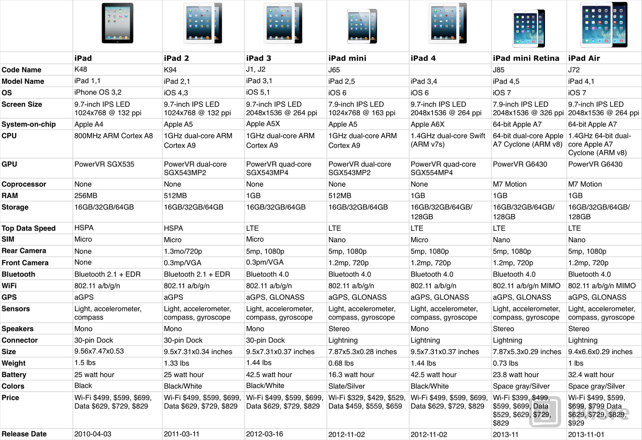
Since Steve Jobs first unveiled it at a special event in 2010, the iPad has improved steadily in one way or another. The iPad 2 was thinner, lighter, and faster. The iPad 3 got a Retina display and LTE. The iPad 4 went Lightning. The iPad mini dropped back to iPad 2 tech, but in a much smaller form factor. The above chart shows the evolution of the iPad from the original to the latest Retina iPad mini and iPad Air, including pricing and capacity at launch. While what you paid for it when you got it might vary, you can check your current model and see how it compares to the ones available now.
iPad Air and Retina iPad mini: Should you upgrade?
When a new iPad hits the market - or two iPads, as is the case right now - one of the hardest decisions we face is whether or not to upgrade from and original iPad, iPad 2, iPad 3, iPad mini, or iPad 4 to the latest and greatest. If you have unlimited funds, you can just buy everything, all the time. Most of us don't, however, so we need to check out the new features of the iPad Air or Retina iPad mini, see how they compare to what we already have, and decide if the difference is worth the price of an entirely new device, a price that starts at $399 and $499 and goes well up from there. So, is there enough value to justify the cost?
How to sell - and get the most money for! - your old iPad before upgrading to an iPad Air or Retina iPad mini
If you plan on upgrading to an iPad Air or Retina iPad mini, selling your old iPad is a no brainer. Apple products hold their resale value very well. If you've taken good care of your iPad, you should have no problem finding it a new home and putting some cash in your pocket while doing it. Selling the old really does help you afford the new. If you're not sure how to sell, or if you just want to make sure you get the most money, or save yourself the most time and effort, possible, here's everything you need to know!
iPad vs. Galaxy vs. Nexus vs. Kindle vs. Surface: Which tablet should you get?
Apple has flipped the tables - er, tablets - and not only managed to cram a 2048x1536 display into the 7.9-inch Retina iPad mini, but managed to cram a full-sized 9.7-inch display into the new iPad Air. But is either of them to right tablet for you? While everyone here at iMore certainly believes the iPad is still the best tablet for most people, most of the time, there are rare exceptions where an alternative tablet might suit your specific needs better. The iPad may have the best overall user experience, the highest quality apps and games, the widest range of services, the biggest selection of accessories, and the best customer support, but there are also things the iPad doesn't offer that other tablets do, like subsidized hardware pricing, digitizer support, Microsoft compatibility, or simply no Apple about them. How do you know which one is for you?
iPad Air vs. MacBook Air: Which Apple portable should you get?
Apple now has two products designated as "Air", the MacBook Air, updated last June with the latest generation Intel Haswell processors, and the brand new iPad Air, introduced in October with a custom Apple A7 chipset. Both are ultra light, super thin, and incredibly long lasting, but one has a keyboard and runs OS X and the other a multitouch and iOS 7. Both can be absolutely killer on a plane, in an office, or around the house. But which one is better for you?
iPad Air vs. Retina iPad mini vs. iPad 2 vs. iPad mini: Which iPad model should you get?
Once you're sure you're buying an iPad and now, the next step is to decide which iPad you're going to get. And this year, it's a tougher decision than ever. The new iPad Air and Retina iPad mini are identical in every way but screen size, 7.9- vs. 9.7-inches the only differentiator. If money is incredibly tight, though the old iPad 2 is a bit cheaper, and the old iPad mini, a cheaper still. No matter which one you choose, however, you'll be paying hundreds of dollars. Either a few, or a lot. So do you go with big or small, old or new? Which iPad should you get?
Silver vs. space gray: Which iPad Air and Retina iPad mini color should you get?
Unlike the pop-art inspired iPhone 5c, Apple's iPad line remains discreetly metallic when it comes to color schemes. It's not as bad as 2010, mind you, when you could have your choice of color, as long as it was black. Now you can get a silver back with white faceplate, or a space gray back with a black faceplate. And you can get either finish on either new iPad, the iPad Air or Retina iPad mini. (The space gray replaces last year's slate gray, likely because it's tougher and easier to anodize.) So which color is better for you?
16GB vs. 32GB vs. 64GB vs. 128GB: Which iPad Air or Retina iPad mini storage capacity should you get?
Apple offers four different storage sized options for the new iPad Air and Retina iPad mini, ranging from a paltry 16GB to an enormous 128GB - literally 8 times the capacity! Every step up in capacity, however, comes with a matching $100 step up in price. That might seem like a pretty straightforward bit of math, but it really isn't! Figuring out how much storage you really need, and how much you can afford is really important. It's the difference between a great experience and a lot of frustration. So what's the deal?
Speed vs. reliability vs. value: Which iPad Air or Retina iPad mini carrier should you get?
AT&T vs. Verizon vs. Sprint vs. T-Mobile in the U.S. Rogers vs. Bell vs. TELUS in Canada. Three vs O2 vs EE vs Vodafone in the U.K. And many more around the world. Then there are various discount carriers, regionals, and MVNOs. It's a mess! How do you know which carrier will give you the fastest data speeds, or the most reliable connections, or simply the best value for your money? It all comes down to where you live, work, or go to school, and what options work best in your specific area. However, there's a lot of broad generalities that can apply. Here are some of the most important, broken down by country!
Apple Store vs. other stores: Where should you buy your iPad Air or Retina iPad mini?
So now that you know what you're getting, how about where? Carrier compatibility aside, the iPad you get will be the same, but the customer service you receive can vary greatly. Also, if you have specific loyalty rewards at a certain carrier or company, that can change the deal you get.
Apple Retail: If you have an Apple Retail Store in your area, you can go there, and if it's in stock, leave with your new iPad right away. They also offer help with your purchase and will even help you get set your new iPhone up free of charge. If you're worried about protecting your investment, they can also get you setup with AppleCare, and their Genius Bar can help you with hardware problems in the future. Corny as it sounds, It's not just shopping, it's an experience. Apple Retail has the best customer service in the business and it shows. There are no discounts, however, not ever. (Though your carrier discounts can still apply.
Apple Online: If there's no Apple Retail store near you there's also Apple Online in many countries. Again, no discounts but you're dealing directly with Apple. If there are any shortages or shipping delays, you can still order and they'll get it out to you as soon as stock allows.
Carrier stores and big box retailers: If you want brick-and-morter but don't have an Apple Store nearby, your carrier will often have one or several stores in your area. If you want a cellular model, drop buy or get it shipped to you. Big box and chain retailers, everything from Best Buy to the Shack to Tesco also carry iPads. If you have loyalty points or they're just super convenient, check them out as well.
Shady operators also try to sell discount iPads, sometimes devices that aren't even really iPads but cheap -- and highly breakable -- knockoffs. It goes without saying you should avoid those. Any deal too good to be true probably is. If you save money only to end up with a phone that doesn't run iOS and may not even run on your carrier you really just wasted your money.
AppleCare+ vs. insurance vs. nothing: Which iPad Air or Retina iPad mini protection plan should you get?
If you plan on picking up a new iPad Air, a Retina iPad mini, or one of the cheaper, previous generation iPads, one of the last - but most important - things you have to decide is whether or not you'd like to get some kind of insurance to protect your investment, whether it be AppleCare+, third party, or something else. There are lots of factors that can play a part in your decision, such as how long you plan on keeping your iPad before upgrading, and how careful you are with it. Here's what you need to know!
If there's any detail you're still not 100% sure about, or any question you'd still love to get answered before you buy your brand new iPad Air or Retina iPad mini, we have fantastic information pages that are always kept up-to-the-minute, and amazing community forums filled with experts for you to talk with. Bookmark them and check back often! And once you've decided, let us know in the comments - which iPad did you get and why?
Good news, folks. A bunch of you have asked us if you can purchase a Nexus 5 from Google Play and activate it on Sprint. We've just heard back from Sprint, and the answer is in the affirmative.
Repeat: Yes, you can purchase a Nexus 5 from Google Play and activate it on Sprint.
Contact: Holly Evarts holly.evarts@columbia.edu 347-453-7408 Columbia University
Columbia Engineers develop new device architecture for 2D materials, making electrical contact from the 1D edge
New York, NYOctober 31, 2013Columbia Engineering researchers have experimentally demonstrated for the first time that it is possible to electrically contact an atomically thin two-dimensional (2D) material only along its one-dimensional (1D) edge, rather than contacting it from the top, which has been the conventional approach. With this new contact architecture, they have developed a new assembly technique for layered materials that prevents contamination at the interfaces, and, using graphene as the model 2D material, show that these two methods in combination result in the cleanest graphene yet realized. The study is published in Science on November 1, 2013.
"This is an exciting new paradigm in materials engineering where instead of the conventional approach of layer by layer growth, hybrid materials can now be fabricated by mechanical assembly of constituent 2D crystals," says Electrical Engineering Professor Ken Shepard, co-author of the paper. "No other group has been able to successfully achieve a pure edge-contact geometry to 2D materials such as graphene."
He adds that earlier efforts have looked at how to improve 'top contacts' by additional engineering such as adding dopants: "Our novel edge-contact geometry provides more efficient contact than the conventional geometry without the need for further complex processing. There are now many more possibilities in the pursuit of both device applications and fundamental physics explorations."
First isolated in 2004, graphene is the best-studied 2D material and has been the subject of thousands of papers studying its electrical behavior and device applications. "But in nearly all of this work, the performance of graphene is degraded by exposure to contamination," notes Mechanical Engineering Professor James Hone who is also a co-author of the study. "It turns out that the problems of contamination and electrical contact are linked. Any high-performance electronic material must be encapsulated in an insulator to protect it from the environment. Graphene lacks the ability to make out-of-plane bonds, which makes electrical contact through its surface difficult, but also prevents bonding to conventional 3D insulators such as oxides. Instead, the best results are obtained by using a 2D insulator, which does not need to make bonds at its surface. However, there has been no way to electrically access a fully-encapsulated graphene sheet until now."
In this work, says Cory Dean, who led the research as a postdoc at Columbia and is now an assistant professor at The City College of New York, the team solved both the contact and contamination problems at once. "One of the greatest assets of 2D materials such as graphene is that being only one atom thick, we have direct access to its electronic properties. At the same time, this can be one of its worst features since this makes the material extremely sensitive to its environment. Any external contamination quickly degrades performance. The need to protect graphene from unwanted disorder, while still allowing electrical access, has been the most significant roadblock preventing development of graphene-based technologies. By making contact only to the 1D edge of graphene, we have developed a fundamentally new way to bridge our 3D world to this fascinating 2D world, without disturbing its inherent properties. This virtually eliminates external contamination and finally allows graphene to show its true potential in electronic devices"
The researchers fully encapsulated the 2D graphene layer in a sandwich of thin insulating boron nitride crystals, employing a new technique in which crystal layers are stacked one-by-one. "Our approach for assembling these heterostructures completely eliminates any contamination between layers," Dean explains, "which we confirmed by cross-sectioning the devices and imaging them in a transmission electron microscope with atomic resolution."
Once they created the stack, they etched it to expose the edge of the graphene layer, and then evaporated metal onto the edge to create the electrical contact. By making contact along the edge, the team realized a 1D interface between the 2D active layer and 3D metal electrode. And, even though electrons entered only at the 1D atomic edge of the graphene sheet, the contact resistance was remarkably low, reaching 100 Ohms per micron of contact widtha value smaller than what can be achieved for contacts at the graphene top surface.
With the two new techniquesthe contact architecture through the 1D edge and the stacking assembly method that prevents contamination at the interfacesthe team was able to produce what they say is the "cleanest graphene yet realized." At room temperature, these devices exhibit previously unachievable performance, including electron mobility at least twice as large as any conventional 2D electron system, and sheet resistivity less than 40 Ohms when sufficient charges are added to the sheet by electrostatic "gating." Amazingly, this 2D sheet resistance corresponds to a "bulk" 3D resistivity smaller than that of any metal at room temperature. At low temperature, electrons travel through the team's samples without scattering, a phenomenon known as ballistic transport. Ballistic transport, had previously been observed in samples close to one micrometer in size, but this work demonstrates the same behavior in samples as large as 20 micrometers. "So far this is limited purely by device size," says Dean, "indicating that the true 'intrinsic' behavior is even better."
The team is now working on applying these techniques to develop new hybrid materials by mechanical assembly and edge contact of hybrid materials drawing from the full suite of available 2D layered materials, including graphene, boron nitride, transition metal dichlcogenides (TMDCs), transition metal oxides (TMOs), and topological insulators (TIs). "We are taking advantage of the unprecedented performance we now routinely achieve in graphene-based devices to explore effects and applications related to ballistic electron transport over fantastically large length scales," Dean adds. "With so much current research focused on developing new devices by integrating layered 2D systems, potential applications are incredible, from vertically structured transistors, tunneling based devices and sensors, photoactive hybrid materials, to flexible and transparent electronics."
"This work results from a wide collaboration of researchers interested in both pure and applied science," says Hone. "The unique environment at Columbia provides an unparalleled opportunity for these two communities to interact and build off one another."
The Columbia team demonstrated the first technique to mechanically layer 2D materials in 2010. These two new techniques, which are critical advancements in the field, are the result of interdisciplinary efforts by Lei Wang (PhD student, Electrical Engineering, Hone group) and Inanc Meric (Postdoc, Electrical Engineering, Shepard group), co-lead authors on this project who worked with the groups of Philip Kim (Physics and Applied Physics and Applied Mathematics, Columbia), James Hone (Mechanical Engineering, Columbia), Ken Shepard (Electrical Engineering, Columbia) and Cory Dean (Physics, City College of New York).
###
This work is supported by the Department of Defense (DoD) through the National Defense Science and Engineering Graduate Fellowship (NDSEG) Program, the National Science Foundation (DMR-1124894), the Air Force Office of Scientific Research (FA9550-09-1-0705), the office of Naval Research (N000141310662), the ONR Grant N000141110633 and the Defense Advanced Research Projects Agency (under ONR Grant N000141210814), and the Nano Material Technology Development Program through the National Research Foundation of Korea (2012M3A7B4049966).
Columbia Engineering
Columbia University's Fu Foundation School of Engineering and Applied Science, founded in 1864, offers programs in nine departments to both undergraduate and graduate students. With facilities specifically designed and equipped to meet the laboratory and research needs of faculty and students, Columbia Engineering is home to NSF-NIH funded centers in genomic science, molecular nanostructures, materials science, and energy, as well as one of the world's leading programs in financial engineering. These interdisciplinary centers are leading the way in their respective fields while individual groups of engineers and scientists collaborate to solve some of modern society's more difficult challenges. http://www.engineering.columbia.edu/
[
| E-mail
Share
]
AAAS and EurekAlert! are not responsible for the accuracy of news releases posted to EurekAlert! by contributing institutions or for the use of any information through the EurekAlert! system.
New techniques produce cleanest graphene yet
PUBLIC RELEASE DATE:
31-Oct-2013
[
| E-mail
]
Share
Contact: Holly Evarts holly.evarts@columbia.edu 347-453-7408 Columbia University
Columbia Engineers develop new device architecture for 2D materials, making electrical contact from the 1D edge
New York, NYOctober 31, 2013Columbia Engineering researchers have experimentally demonstrated for the first time that it is possible to electrically contact an atomically thin two-dimensional (2D) material only along its one-dimensional (1D) edge, rather than contacting it from the top, which has been the conventional approach. With this new contact architecture, they have developed a new assembly technique for layered materials that prevents contamination at the interfaces, and, using graphene as the model 2D material, show that these two methods in combination result in the cleanest graphene yet realized. The study is published in Science on November 1, 2013.
"This is an exciting new paradigm in materials engineering where instead of the conventional approach of layer by layer growth, hybrid materials can now be fabricated by mechanical assembly of constituent 2D crystals," says Electrical Engineering Professor Ken Shepard, co-author of the paper. "No other group has been able to successfully achieve a pure edge-contact geometry to 2D materials such as graphene."
He adds that earlier efforts have looked at how to improve 'top contacts' by additional engineering such as adding dopants: "Our novel edge-contact geometry provides more efficient contact than the conventional geometry without the need for further complex processing. There are now many more possibilities in the pursuit of both device applications and fundamental physics explorations."
First isolated in 2004, graphene is the best-studied 2D material and has been the subject of thousands of papers studying its electrical behavior and device applications. "But in nearly all of this work, the performance of graphene is degraded by exposure to contamination," notes Mechanical Engineering Professor James Hone who is also a co-author of the study. "It turns out that the problems of contamination and electrical contact are linked. Any high-performance electronic material must be encapsulated in an insulator to protect it from the environment. Graphene lacks the ability to make out-of-plane bonds, which makes electrical contact through its surface difficult, but also prevents bonding to conventional 3D insulators such as oxides. Instead, the best results are obtained by using a 2D insulator, which does not need to make bonds at its surface. However, there has been no way to electrically access a fully-encapsulated graphene sheet until now."
In this work, says Cory Dean, who led the research as a postdoc at Columbia and is now an assistant professor at The City College of New York, the team solved both the contact and contamination problems at once. "One of the greatest assets of 2D materials such as graphene is that being only one atom thick, we have direct access to its electronic properties. At the same time, this can be one of its worst features since this makes the material extremely sensitive to its environment. Any external contamination quickly degrades performance. The need to protect graphene from unwanted disorder, while still allowing electrical access, has been the most significant roadblock preventing development of graphene-based technologies. By making contact only to the 1D edge of graphene, we have developed a fundamentally new way to bridge our 3D world to this fascinating 2D world, without disturbing its inherent properties. This virtually eliminates external contamination and finally allows graphene to show its true potential in electronic devices"
The researchers fully encapsulated the 2D graphene layer in a sandwich of thin insulating boron nitride crystals, employing a new technique in which crystal layers are stacked one-by-one. "Our approach for assembling these heterostructures completely eliminates any contamination between layers," Dean explains, "which we confirmed by cross-sectioning the devices and imaging them in a transmission electron microscope with atomic resolution."
Once they created the stack, they etched it to expose the edge of the graphene layer, and then evaporated metal onto the edge to create the electrical contact. By making contact along the edge, the team realized a 1D interface between the 2D active layer and 3D metal electrode. And, even though electrons entered only at the 1D atomic edge of the graphene sheet, the contact resistance was remarkably low, reaching 100 Ohms per micron of contact widtha value smaller than what can be achieved for contacts at the graphene top surface.
With the two new techniquesthe contact architecture through the 1D edge and the stacking assembly method that prevents contamination at the interfacesthe team was able to produce what they say is the "cleanest graphene yet realized." At room temperature, these devices exhibit previously unachievable performance, including electron mobility at least twice as large as any conventional 2D electron system, and sheet resistivity less than 40 Ohms when sufficient charges are added to the sheet by electrostatic "gating." Amazingly, this 2D sheet resistance corresponds to a "bulk" 3D resistivity smaller than that of any metal at room temperature. At low temperature, electrons travel through the team's samples without scattering, a phenomenon known as ballistic transport. Ballistic transport, had previously been observed in samples close to one micrometer in size, but this work demonstrates the same behavior in samples as large as 20 micrometers. "So far this is limited purely by device size," says Dean, "indicating that the true 'intrinsic' behavior is even better."
The team is now working on applying these techniques to develop new hybrid materials by mechanical assembly and edge contact of hybrid materials drawing from the full suite of available 2D layered materials, including graphene, boron nitride, transition metal dichlcogenides (TMDCs), transition metal oxides (TMOs), and topological insulators (TIs). "We are taking advantage of the unprecedented performance we now routinely achieve in graphene-based devices to explore effects and applications related to ballistic electron transport over fantastically large length scales," Dean adds. "With so much current research focused on developing new devices by integrating layered 2D systems, potential applications are incredible, from vertically structured transistors, tunneling based devices and sensors, photoactive hybrid materials, to flexible and transparent electronics."
"This work results from a wide collaboration of researchers interested in both pure and applied science," says Hone. "The unique environment at Columbia provides an unparalleled opportunity for these two communities to interact and build off one another."
The Columbia team demonstrated the first technique to mechanically layer 2D materials in 2010. These two new techniques, which are critical advancements in the field, are the result of interdisciplinary efforts by Lei Wang (PhD student, Electrical Engineering, Hone group) and Inanc Meric (Postdoc, Electrical Engineering, Shepard group), co-lead authors on this project who worked with the groups of Philip Kim (Physics and Applied Physics and Applied Mathematics, Columbia), James Hone (Mechanical Engineering, Columbia), Ken Shepard (Electrical Engineering, Columbia) and Cory Dean (Physics, City College of New York).
###
This work is supported by the Department of Defense (DoD) through the National Defense Science and Engineering Graduate Fellowship (NDSEG) Program, the National Science Foundation (DMR-1124894), the Air Force Office of Scientific Research (FA9550-09-1-0705), the office of Naval Research (N000141310662), the ONR Grant N000141110633 and the Defense Advanced Research Projects Agency (under ONR Grant N000141210814), and the Nano Material Technology Development Program through the National Research Foundation of Korea (2012M3A7B4049966).
Columbia Engineering
Columbia University's Fu Foundation School of Engineering and Applied Science, founded in 1864, offers programs in nine departments to both undergraduate and graduate students. With facilities specifically designed and equipped to meet the laboratory and research needs of faculty and students, Columbia Engineering is home to NSF-NIH funded centers in genomic science, molecular nanostructures, materials science, and energy, as well as one of the world's leading programs in financial engineering. These interdisciplinary centers are leading the way in their respective fields while individual groups of engineers and scientists collaborate to solve some of modern society's more difficult challenges. http://www.engineering.columbia.edu/
[
| E-mail
Share
]
AAAS and EurekAlert! are not responsible for the accuracy of news releases posted to EurekAlert! by contributing institutions or for the use of any information through the EurekAlert! system.